Our group combines experimental and theoretical approaches and draws knowledge from a breadth of disciplines (physical and computing sciences, engineering, and applied mathematics) to explore the challenging intellectual or practical questions that arise in using nanoscale and when connecting large scales, such as those of massively integrated electronic systems - a complex system, to small scales, such as those of small devices and structures that come about from the use of nanoscale. In the former, we invent, develop new technologies, new applications and understanding. The latter, because of non-linearities, coupling across scales, hierarchy and adaptation, is an exciting area at the boundaries of science and engineering; we have started calling this NanoComplexity. Our effort encompasses electronics, optics, creation of new technologies, information processing and communications. In detail, our group has spent the past few years exploring adaptive energy-efficient electronics - a path that leads through small devices and their new circuits, newer approaches to CMOS structures, three-dimensional integration, mixed-signal electronics, ideas and technologies that allow functional integration, and also interesting offshoots for small structures in other interdisciplinary areas. Nanoscale and energy constraints have led us now to explore directions for computation that are approximate but useful and robust.
Some directions of our effort:
-
Nanoscale Devices
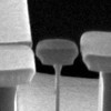
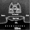
Nanoscale brings together a variety of interesting changes in properties, some useful and some not for electrosciences in that region that bridges the atom to bulk. In electronics, many properties improve, such as current capability or transistor speed, or makes tunneling significant - useful in floating gate or nanocrystal memories, and many deteriorate, tunneling can also become a source of leakage and unnecessary power dissipation, and power in increasingly smaller areas leads to power dissipation. Use of smaller structures also means increase in statistical variance in devices. Our past efforts have resulted in the inventions of nanocrystal, quantum-dot and back-storage memories, fast adaptive transistors with separately gated double gates, fluidic transistors for molecular profiling, world-record low current quantum wire lasers, development of new technologies, and understanding of a variety of devices and phenomena such as random telegraph signal in nanoscale memories. Our current efforts look at new directions that promise a way around many of the debilitating effects of nanoscale. -
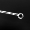
Nanowires and Photoelectric Conversion
Photoelectric energy conversion at low environment and financial cost is very desirable and numerous approaches are being tried around the world using inorganic and organic materials - semiconducting as well as others. Current silicon photovoltaics using an abundantly available material achieves electric energy costs that are still many times higher than that from traditional energy sources. A lot of this is due to the cost of wafers or the high temperature and costly fabrication processes employed. We have invented and employed growth of single crystal wires on cheap surfaces to make solar cells. We are working on improving these solar cells and we employ a variety of characterization techniques to study the properties of materials and their interfaces. We are also exploring this approach to obtain light sources. We collaborate in this effort with Prof. Jiwoong Park's group in Chemistry at Cornell, Dr. Supratik Guha at IBM Research and Prof. Venky Narayanamurti's group at Harvard University. -
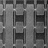
New Approaches to Nanoscale Patterning
Patterning nanoscale at low defect rates where the structure is customized, i.e. when external information is programmed in at the smallest dimensions such as in wiring or placement on an integrated circuit or of the device pattern itself, is a major technological challenge. Lithography with reasonable speeds is incredibly expensive, and statistical effects again become a problem (variance in number of photons and electrons, or of molecules of the resists and their edge pattern). We are exploring approaches for extremely low cost directed lithography without resorting to use of photons or electrons, but by directed self-assembly that promises to achieve precision of electron-beam lithography at very high speeds and at costs significantly lower than that of optical lithography. -
Self-Assembly for Devices
The traditional approach of making most electronic devices is to define the smallest dimension by lithography. So, for 10 or 20 nm dimensions, we must define a dimension close to this for pattern transfer, an approach that traditionally runs into the problems outlined above. There are possibly ways around this by taking a much larger dimension of a device, and achieve the rest of the smaller dimensions within it, using the self-assembly approaches developed by the chemists and materials scientists. Starting from the largest dimension of a transistor, we are fabricating the rest of the structure using self-assembly techniques. In this effort, we work closely with Prof. Chris Ober's group in Materials Science and Dr. Chuck Black at Brookhaven National Laboratory. -
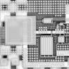
Three-Dimensional Integration, Circuits and Communications
Electronics today integrates a large number of technologies - fabrication approaches, devices with different functions, different materials, and wired interconnects. All of this complicates the technologies employed and potentially increases delay and dissipation arising in moving information around. Three-dimensional integration offers potential opportunities beyond traditional miniaturization in a number of application areas by at least shortening path lengths. In the past, we have developed technologies that have allowed us to interconnect devices across four device layers, analyzed floor planning and memory-logic integration for achieving highest processor performance, with Lincoln Labs fabricated the first three-dimensional microprocessor - a very simple 8 bit implementation, and looked at thermal issues. Our current interest is in finding architectural approaches that provide a way around the limited fan-in and fan-out of wired approaches, by looking at wireless means for communications for integrated three-dimensional systems environment. We also continue to explore adaptive circuit techniques. One direction of practical importance is achieving desired performance characteristics while minimizing power in the presence of the increased variabilities encountered at nanoscale. For this, we employ separately gated self-aligned double gate transistors that we developed in an earlier effort. We collaborate in this effort with Dr. Paul Solomon at IBM Research. -
Inexact Computing
The current digital approach to computing, in essence, is based on sequential processing using linearized approaches that are implemented in a Turing model. Our circuits are designed to be correct. A low error rate (imagine trillions of elements all operating correctly in a physical approach that has statistical distribution) implies large activation energies, and to get a reasonable speed with sequential approaches, large power. Most problems of interest, those that do not involve precision of numbers such as in finance, do not need this degree of correctness. Most inputs are shades of gray (inputs that are ‘most probably’ this or that). Most complex problems can employ approaches that are statistical in origin, even circuits can be probabilistic, to tremendously reduce the power and achieve useful answers. We are employing ideas from across the sciences to find approaches that can allow us to lower energy by many orders of magnitude while allowing computing with variable devices. -
Complex Systems
If one could make devices with a minimum dimension of 10 nm, potentially a terascale density of devices is possible on a planar integrated circuit - several orders of magnitude larger than today. This is a sea of devices where current techniques of architecture, design of circuits and devices for worst case conditions, or the approaches to networks that pass around the information cannot be as practiced today. Power and costs for special purpose designs will be prohibitive. Only a miniscule percentage of the devices can be operational at any given moment, devices will have dynamic changes and software will often break while in use. How and what can one robustly accomplish in such an environment? We are looking at how ideas from statistical physics, dynamic configuration approaches with built in self-testing, network theory, probabilistic approaches, appropriate hardware technologies, etc. can be brought together coherently to make this terascale complex system useful.